Custom Membrane Switches & Backlit Keypads
Engineered human-machine interface (HMI) solutions manufactured under strict ISO 9001 and Intertek quality standards.
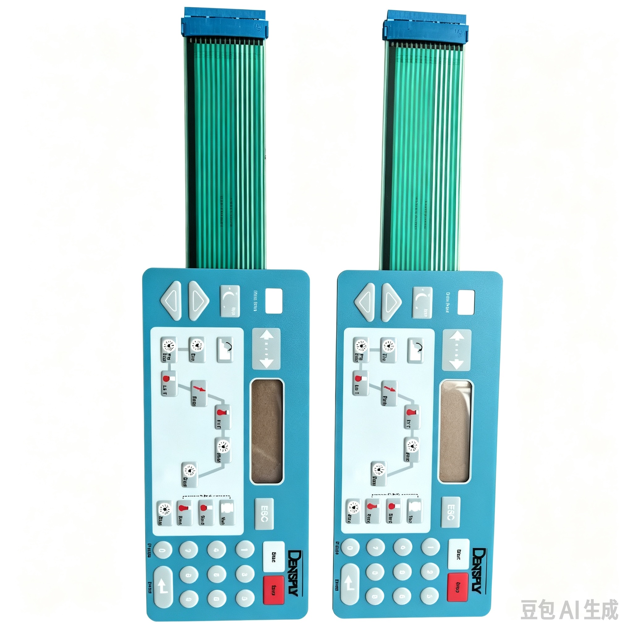
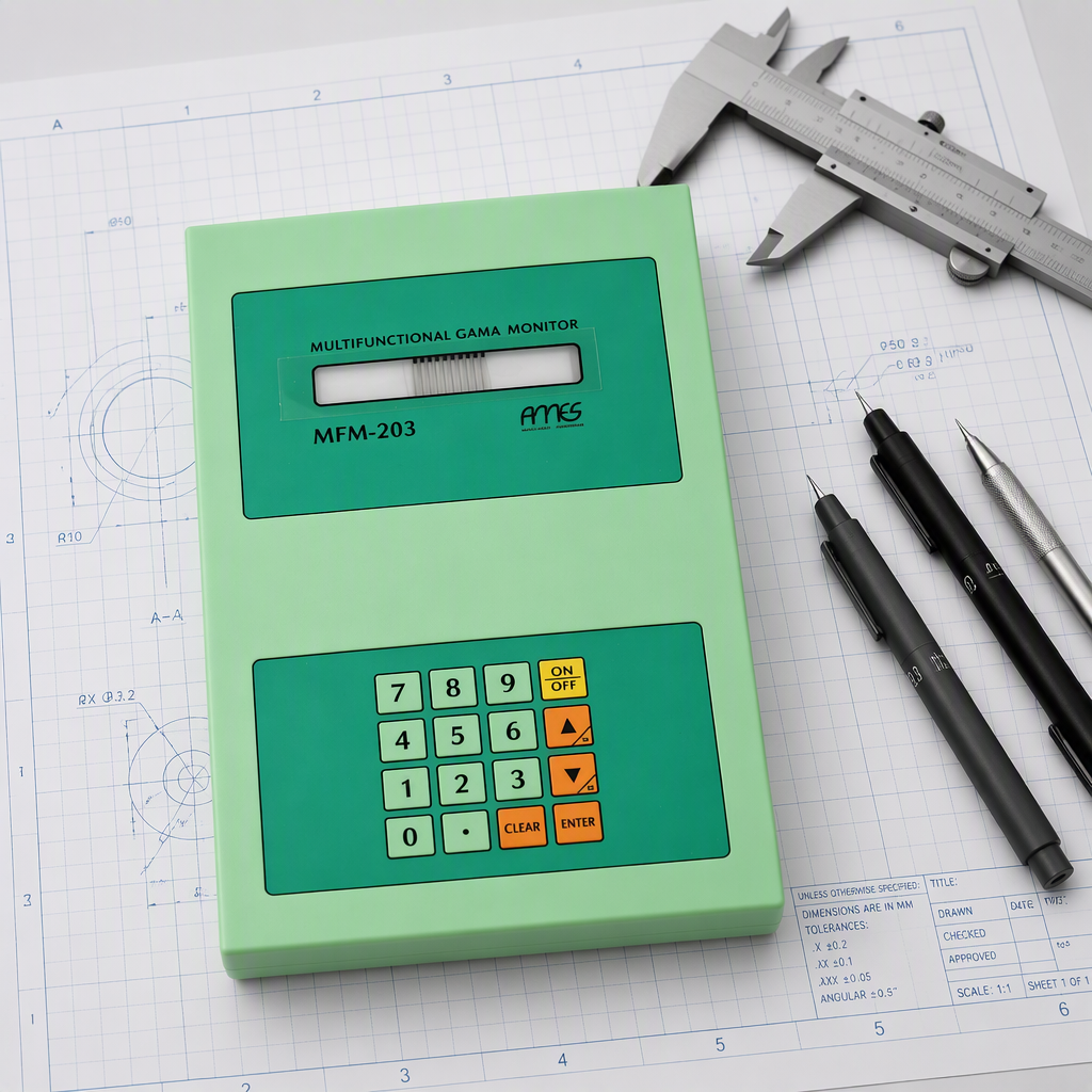
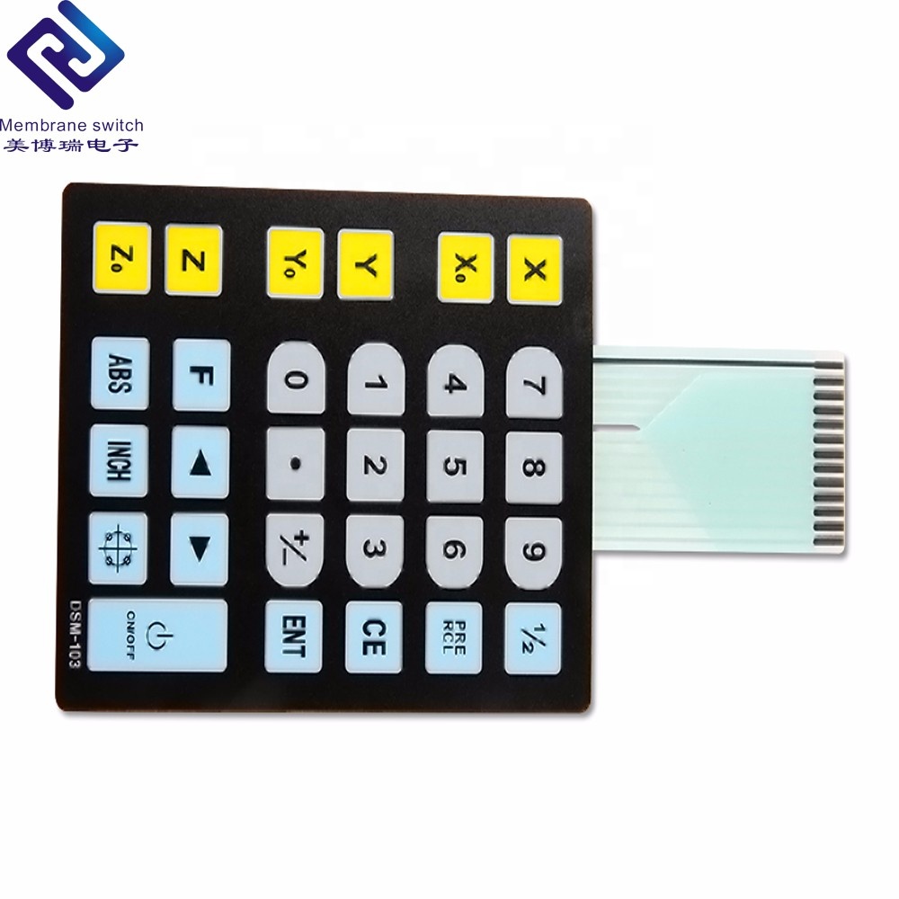
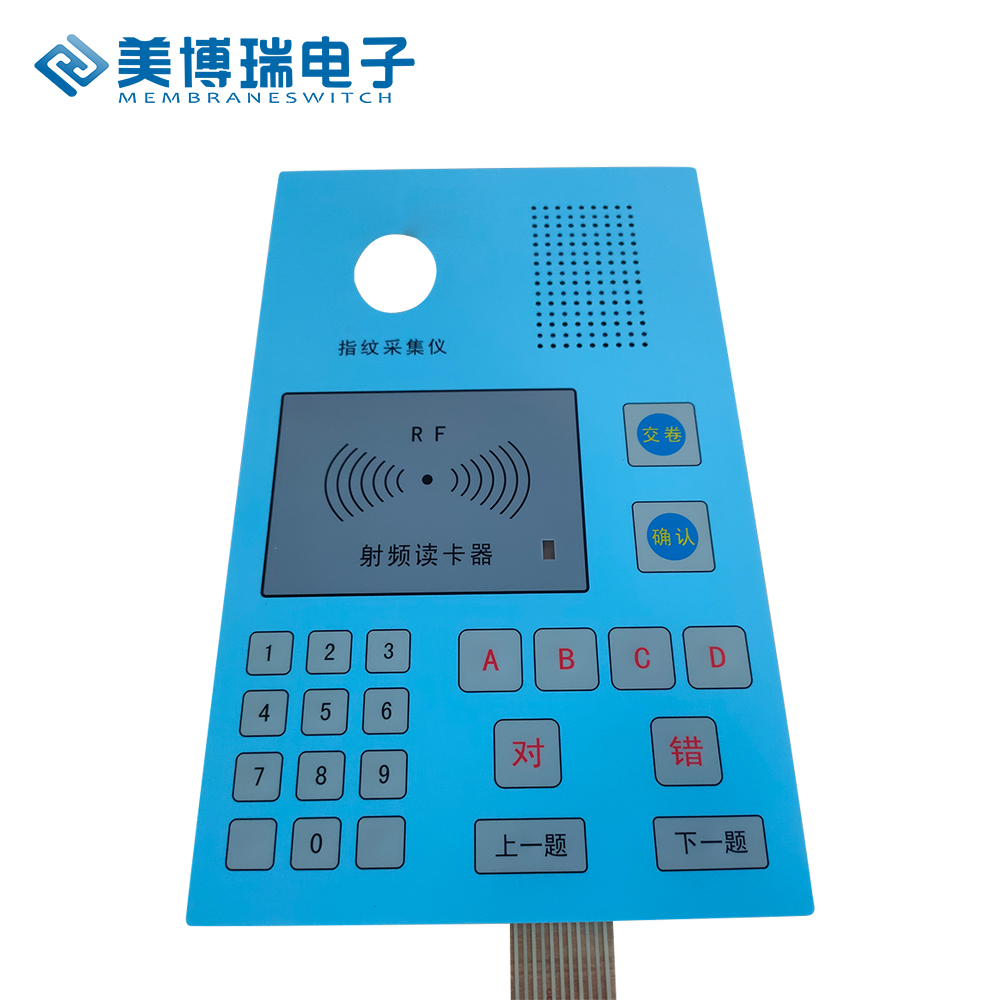
1. Executive Overview: Electroluminescent (EL) Backlighting in Modern HMI
In the evolving architecture of Human-Machine Interfaces (HMI), visual feedback and low-light operation remain imperative across medical devices, industrial automation systems, military consoles, automotive dashboards, and high-tier consumer electronics. Electroluminescent (EL) backlit panels are solid-state, ultra-thin luminescent structures that emit light when excited by an alternating electrical current (AC). Unlike traditional light sources such as incandescent lamps or point-source LED arrays, EL panels generate a perfectly uniform, surface-emitting "cold" light without heat generation, optical hotspotting, or substantial spatial volume.
An EL backlit panel operates via phosphor particles (typically copper-doped zinc sulfide, ZnS:Cu) encapsulated between two conductive electrodes—one of which is optically transparent (Indium Tin Oxide, ITO). When an alternating current (typically 80V–120V AC at 400Hz–1kHz) is applied, the high electric field excites the phosphor electrons, resulting in electroluminescence. For global procurement officers and electronic engineers searching for top 10 EL backlit panel factories, evaluating technical capabilities requires looking beyond basic price-per-square-inch metrics. Crucial parameters include dielectric breakdown resilience, phosphor decay half-life, moisture barrier integrity, and inverter circuit matching.
Top 10 EL Backlit Panel Factories & Sourcing Benchmark
A global benchmark comparing key manufacturing hubs across technical competency, quality management systems, and customization capabilities.
When engineering procurement teams conduct global audits for EL panel suppliers, manufacturers are typically categorized into four main regional paradigms: East Asian high-precision clusters (China Mainland & Taiwan), European high-reliability specialists (Germany & Switzerland), and North American niche defense suppliers. Below is a comparative structural overview of the top factory tiers in the market today.
| Factory Tier / Region | Primary Strengths | Typical Lead Time | ISO / Quality Certs | Best Suited Applications |
|---|---|---|---|---|
| TAVO / MEIBORUI (China) | In-house 37 printing lines, German tech partnership, full HMI/FPC integration | 1–2 Weeks (Samples) 2–3 Weeks (Mass) |
ISO 9001, Intertek Assessed, IP67 Testing | Industrial Automation, Medical, Telecommunication, Appliances |
| Tier-1 Taiwan Manufacturers | High automation, advanced optoelectronics R&D | 3–4 Weeks | ISO 9001, IATF 16949 | Automotive instrument panels, aviation avionics |
| European Specialized Labs | Custom military-grade specs, extreme temperature rating | 6–8 Weeks | ISO 9001, EN 9100 | Defense, aerospace, heavy rail locomotion |
| US Electronics Integrators | Domestic defense compliance (ITAR), local engineering support | 4–6 Weeks | ISO 9001, AS9100D | Medical diagnostics, aerospace ground equipment |
| Standard Asian OEM Factories | Low cost for simple high-volume consumer goods | 2–4 Weeks | ISO 9001 | Basic consumer novelty lighting, static backlit toys |
Phosphor Layer Uniformity
Top factories utilize micro-meter controlled silkscreen tension and automatic ink dosing to ensure phosphor thickness variance remains within ±3 microns across the entire panel surface.
Environmental Sealing
Humidity is the primary enemy of EL phosphor. Leading factories encapsulate the light engine between fluoropolymer or moisture-barrier PET films using heat-seal lamination.
Inverter Optimization
Matching the capacitance of the EL panel (measured in nanofarads) to dedicated AC driver circuitry guarantees peak luminescence while extending operating half-life beyond 5,000–10,000 hours.
2. Engineering Deep-Dive: Material Science & EL Panel Layer Architecture
Understanding the internal structure of an electroluminescent panel is essential for design engineers drafting product specifications. Unlike rigid backlight units, an EL panel is constructed as a flexible, multi-layered sandwich through consecutive screen-printing or coating processes.
Transparent Substrate & ITO
Optical-grade PET film sputtered with a ultra-thin layer of Indium Tin Oxide (ITO) serving as the front transparent conductive anode.
Electroluminescent Layer
High-purity zinc sulfide (ZnS) phosphors suspended in a high-dielectric resin matrix, determining light color (blue-green, white, orange).
Dielectric Insulating Layer
Barium titanate (BaTiO3) reflective dielectric layer that prevents electrical arc breakdown and reflects emitted photons forward.
Rear Cathode & Busbar
Conductive silver/carbon ink printed as the rear electrode, terminated with silver busbars and crimped connector pins or pitch flex tails.
Photometric & Electrical Performance Metrics
When defining technical requirements for custom EL backlit panels or hybrid membrane keypads, engineers must specify key operating envelope constraints:
- Luminance Output: Typical initial brightness ranges between 30 cd/m² and 120 cd/m² depending on driving voltage (80V–150V RMS) and excitation frequency (400Hz–2000Hz).
- Power Consumption: Highly efficient solid-state excitation consuming only 0.2mW/cm² to 1.2mW/cm², making EL backlighting ideal for battery-operated portable devices.
- Operating Temperature Spectrum: Exceptional thermal resilience ranging from -30°C to +70°C without color shift or liquid crystal freezing issues encountered in displays.
- Panel Thickness: Ultra-thin form factor of 0.25mm to 0.45mm allows mounting beneath graphic overlays without increasing tactile travel distance.
EL Backlit Panels vs. Light Guide Film (LGF) vs. Direct LED Arrays
Selecting the optimal backlighting technology for membrane switches, touch keypads, and industrial control panels.
| Evaluation Parameter | EL Backlit Panel (Electroluminescent) | Light Guide Film (LGF) + Side LEDs | Direct Matrix LED Array |
|---|---|---|---|
| Illumination Uniformity | 100% Uniform Surface Light (No Hotspots) | 80% – 90% Uniformity (Requires micro-dots) | Low to Moderate (Point sources cause hot spots) |
| Assembly Thickness | Ultra Thin (0.25mm – 0.40mm) | Thin (0.50mm – 0.80mm) | Thick (2.5mm – 5.0mm+ requiring spacer cavities) |
| Power Source Required | AC Inverter Driver (80V-110V AC, 400Hz+) | Standard Low-Voltage DC (2V–3.3V DC) | Standard Low-Voltage DC (5V–12V DC) |
| Heat Generation | Zero Heat ("Cold Light Source") | Low Heat from side LEDs | Moderate to High Heat (Thermal management required) |
| Operating Lifespan (Half-Life) | 5,000 – 10,000 Hours (Gradual decay) | 30,000 – 50,000 Hours | 50,000+ Hours |
| Selective Zone Control | Yes (Screen-printed isolated phosphors) | Moderate (Light barriers required) | Excellent (Individual pixel/key addressability) |
| Tooling & Setup Cost | Economical Silkscreen Tooling | Precision Optical Injection / Stamping Tooling | Low Tooling (Standard PCB SMT trace design) |
3. Future Procurement & Technology Trends in Backlit HMI Panels (2025–2030)
As human-machine interaction transitions toward sleeker, smarter, and more responsive interfaces, the global market for EL panels and backlit membrane switches is experiencing significant technological transformations. Sourcing directors and product design engineers must consider these emerging industry trends when planning next-generation equipment builds:
Trend 1: Hybrid EL-Capacitive Sensing Integration
Traditional membrane keypads relied exclusively on mechanical tactile switches (metal domes or poly domes). Modern industrial and medical design trends favor seamless, easy-to-clean glass or PC surfaces. Leading factories are combining EL backlighting with capacitive touch sensing layers on a single FPC flex circuit or ITO substrate. This provides a completely flat interface, illuminated icon feedback, and zero-force touch sensing in a single assembly under 1.0mm thickness.
Trend 2: Eco-Friendly Water-Based Phosphor Inks & RoHS3 Compliance
Global environmental regulations, including EU REACH and RoHS3, are enforcing stricter limits on volatile organic compounds (VOCs) and heavy metal additives used in luminescent inks. Advanced EL factories have revamped chemical formulations, replacing solvent-heavy dielectric resins with water-based micro-encapsulated phosphor vehicles. These new materials yield higher initial brightness while adhering to stringent green manufacturing certifications.
Trend 3: Smart Micro-Inverters with Automatic Frequency Tuning
Historically, one drawback of EL panels was the acoustic hum or power inefficiency resulting from poorly matched third-party inverters. Next-generation HMI assemblies integrate surface-mount (SMT) micro-inverters directly onto the rear PCB or FPC tail of the keypad. These smart driver ICs feature automatic load-sensing that dynamically adjusts frequency as the EL panel ages, maintaining constant luminance while extending operational lifespan by up to 40%.
Trend 4: Smart Light Guide Film (LGF) & EL Co-Existence
Rather than viewing LGF and EL as mutually exclusive technologies, high-tier HMI design teams now combine both. For static background icon backlighting, ultra-thin EL panels provide perfect surface uniformity. For dynamic status indicators requiring multi-color RGB changes, integrated LGF strips powered by side-firing SMT LEDs are embedded into adjacent zones of the same membrane assembly.
Why TAVO / MEIBORUI Leads in Custom HMI & Backlit Solutions
Over three decades of manufacturing excellence, combining advanced cleanroom processing, German technology collaboration, and complete vertical integration.
Vertical In-House Production
From initial CAD artwork conversion, precision film output, and screen printing (37 lines) to digital UV printing (Mimaki), laser cutting, and final circuit testing, every production step is performed inside our own facilities.
Dual Production Bases
Operating dual processing bases in Xianghe Economic Development Zone (Hebei) and Huizhou (Guangdong) spanning over 2,219 m². Production capacity is optimized dynamically to ensure zero lead-time bottlenecks.
Rigorous Quality Assurance
ISO 9001 quality system verified onsite by Intertek. Comprehensive testing includes automated computer circuit testing, actuation life-cycle testers, salt fog chambers, and xenon lamp UV aging chambers.
Proven Global Partnerships & Technical Lineage
Tracing our membrane switch and keypad processing lineage back to 1990, TAVO has established long-term technical cooperation with German engineering partners, continuously upgrading screen printing technology, optical bonding techniques (OCA), and light guide film integration. Our custom HMI solutions are deployed globally across high-reliability sectors, including Siemens industrial equipment, ABB control units, Haier smart home appliances, high-speed rail locomotion consoles, and medical diagnostic instruments.
Frequently Asked Questions (FAQ) for EL & Backlit Sourcing
Key technical answers to assist engineering and procurement teams in evaluating customized EL panels and membrane switch keypads.
What engineering files and specifications are required to initiate a custom EL backlit panel quote?
- Dimensional Outline Drawing: Vector files (CAD .DXF, .DWG, Adobe Illustrator .AI, or vector .PDF) showing panel dimensions, window cutouts, and tail location.
- Graphic Artwork & Color Scheme: Pantone color codes for overlay graphics and specified translucent zones for backlighting.
- Illumination Specifications: Desired illuminated area, target brightness (cd/m²), ambient operating conditions, and available input power supply (DC voltage available to power the AC inverter driver).
- Switch & Electrical Schematic: Circuit pin-out matrix, tail connector type (e.g., 2.54mm pitch female header, ZIF flex contact), and tactile dome feedback requirements.
How does an EL panel compare to LGF (Light Guide Film) in terms of tooling costs and lead times?
What causes EL panel brightness degradation, and how do top factories mitigate it?
Can EL backlit panels be combined with waterproof IP65/IP67 membrane switch keypads?
Does TAVO support prototype development and low-volume initial production runs?
Request Engineering Consultation & Factory Quote
Partner with an ISO 9001 certified custom membrane switch and EL panel manufacturer. Our senior engineering team will evaluate your technical drawing, optimize stack-up layers, and deliver a competitive factory-direct proposal within 24 hours.