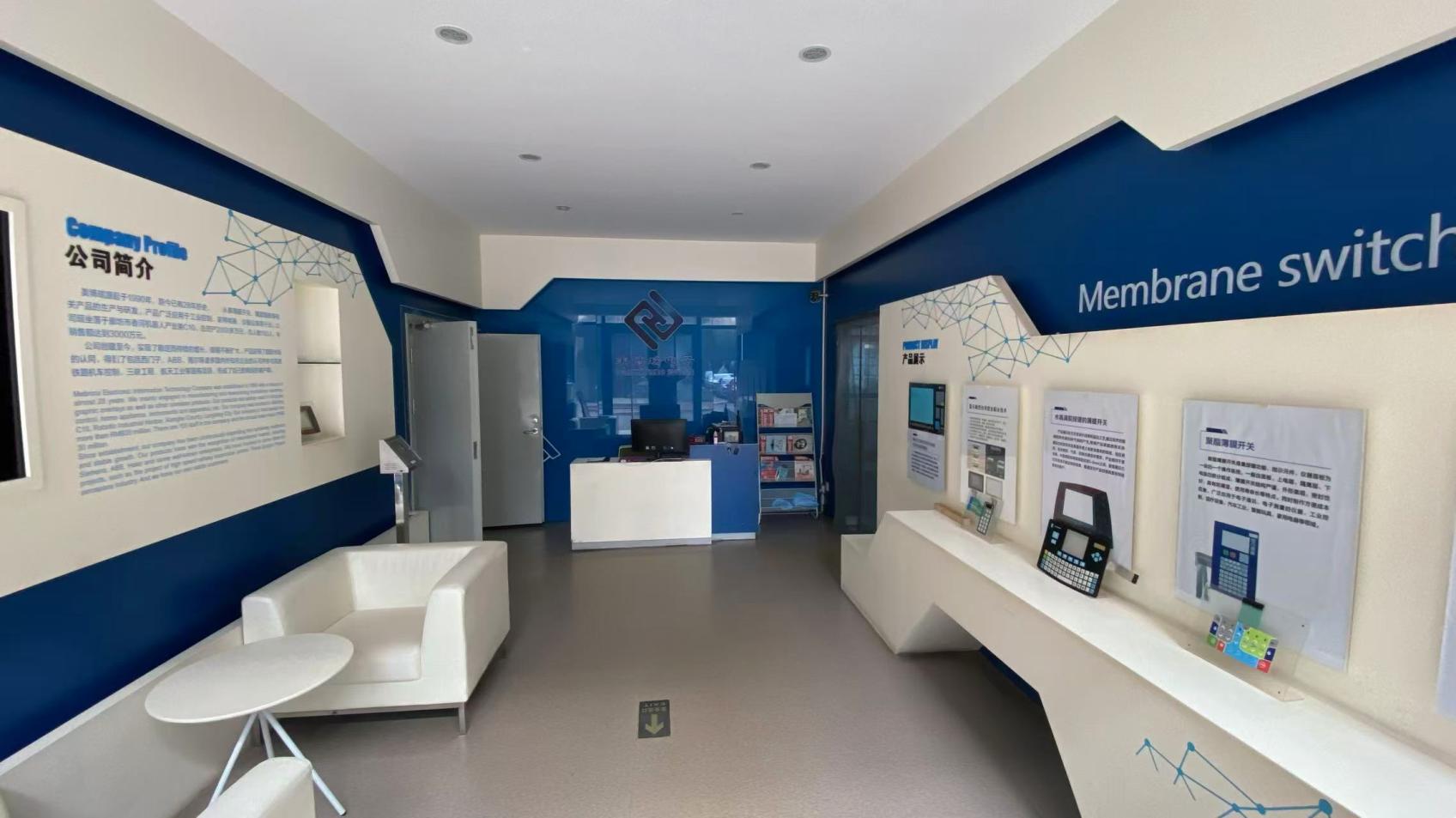
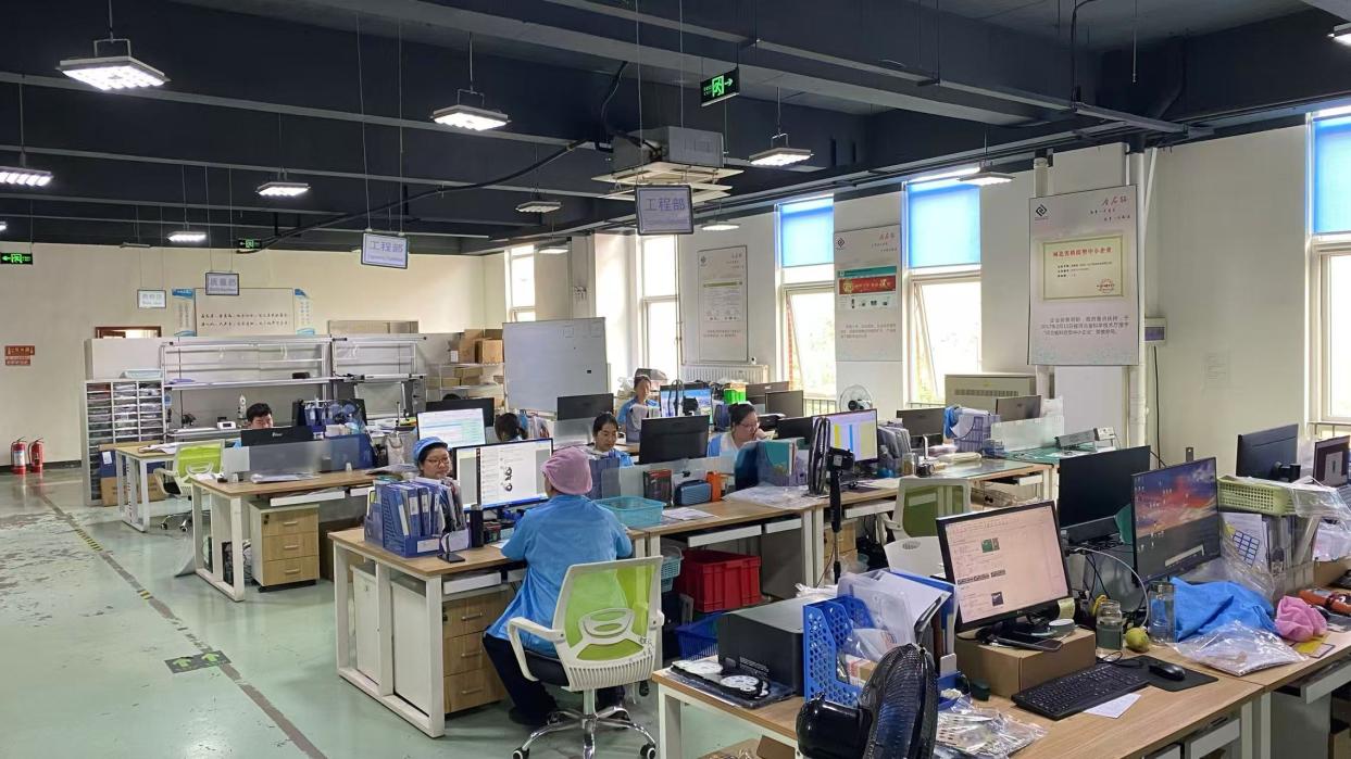
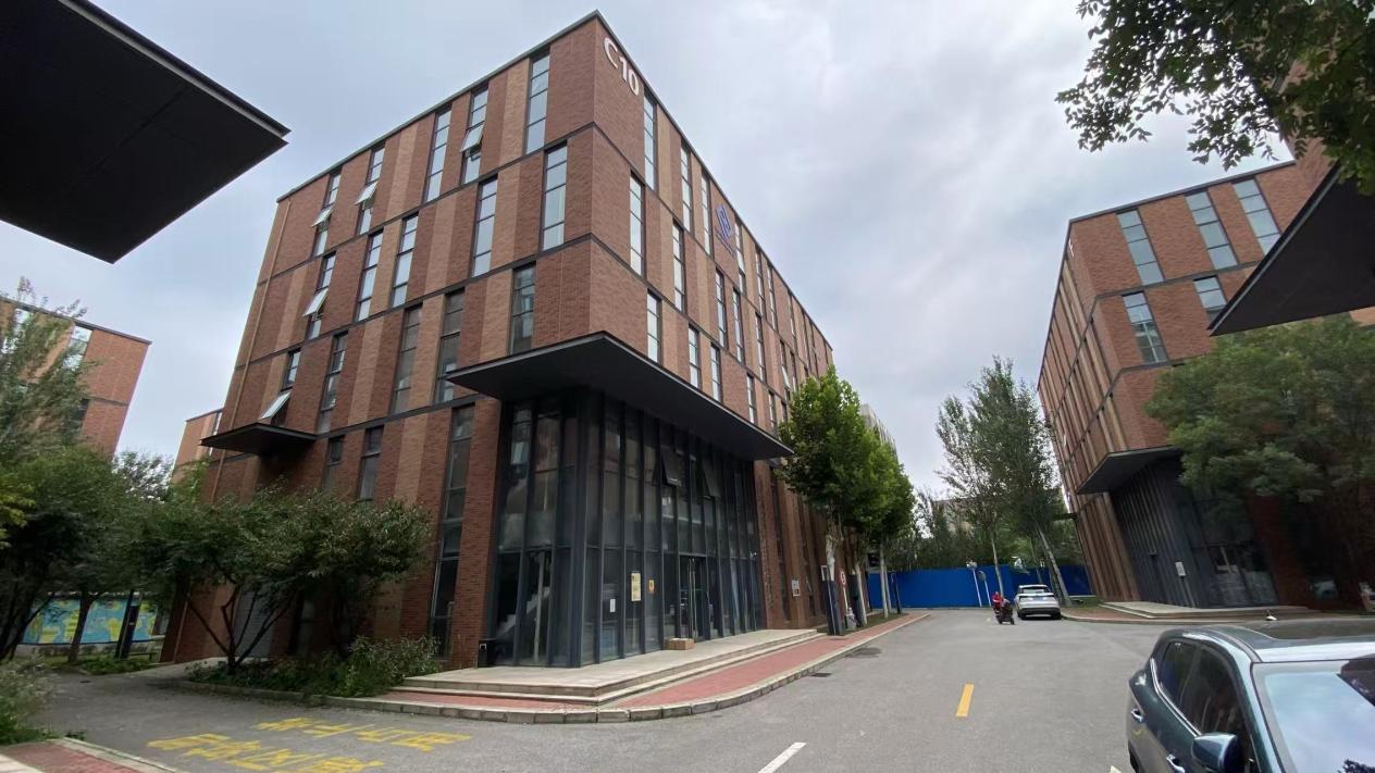
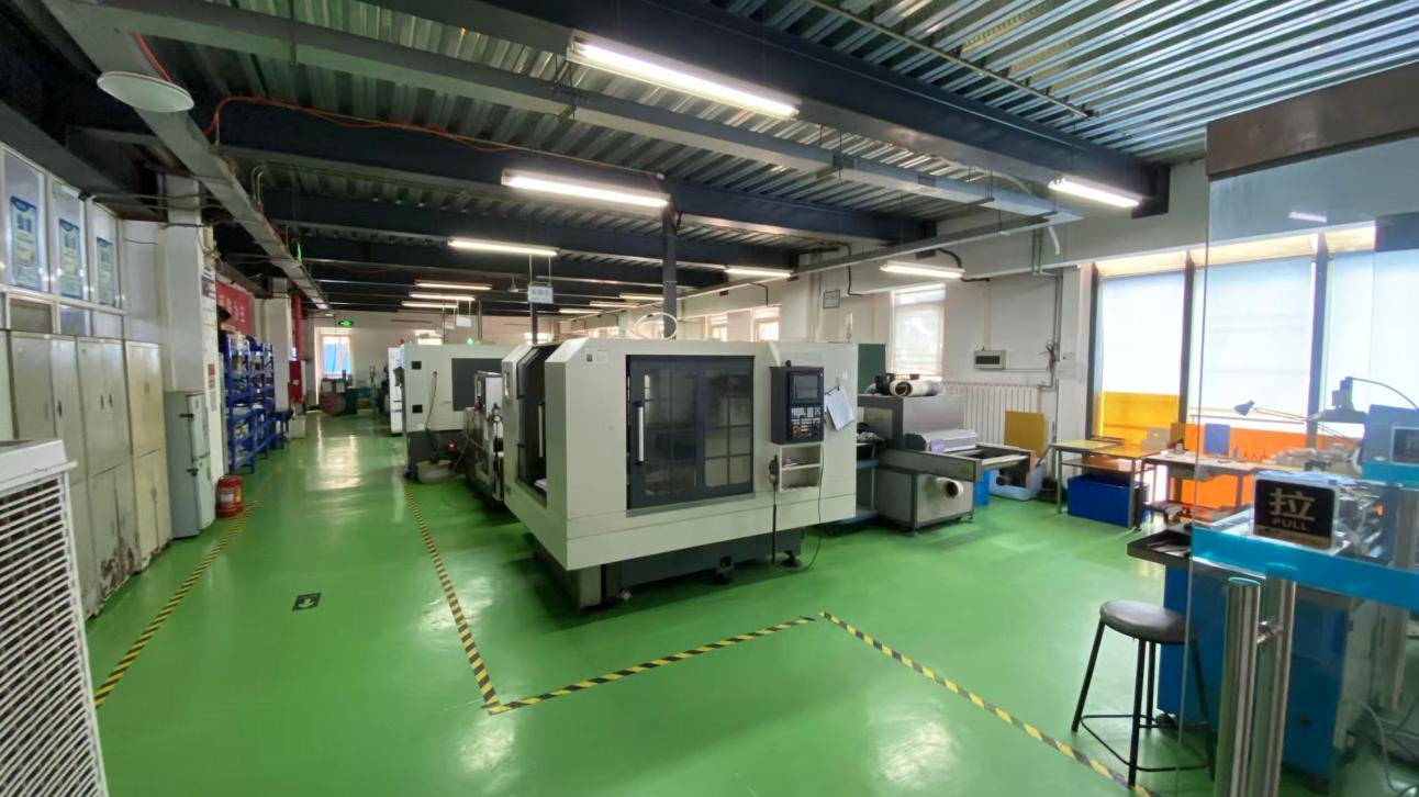
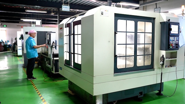
Flexible Printed Circuit Board automated manufacturing line
Precision laser profiling and etching of flexible printed circuits
Multilayer Flexible Printed Circuit Board assembly line
Optical and dimensional verification of Flexible Printed Circuit Boards
Technical Sourcing & Engineering Whitepaper

Flexible Printed Circuit Board: The Complete Sourcing, Engineering & DFM Architecture Guide for Global OEM Buyers

In modern high-reliability electronics, human-machine interfaces, and electromechanical systems, the Flexible Printed Circuit Board (commonly referred to as FPC or flex circuit) has transitioned from an optional packaging alternative to an indispensable structural backbone. Unlike traditional rigid printed circuit boards or screen-printed silver-conductor membranes, a Flexible Printed Circuit Board utilizes rolled annealed (RA) or electro-deposited (ED) copper foil permanently bonded to polyimide (PI) dielectric films, delivering unmatched dynamic flex endurance, ultra-compact three-dimensional routing, and resilient electrical stability.

As global original equipment manufacturers (OEMs) demand higher signal integrity, micro-pitch component integration, and weight reduction across industrial automation, medical robotics, high-speed rail systems, and aerospace avionics, navigating the technical landscape of flexible circuits requires authoritative design-for-manufacturability (DFM) insight. TAVO Electronic Information Technology Co., Ltd. provides decades of specialized fabrication mastery, translating complex schematics into robust, space-optimized flexible circuit interconnects.

  • Copper conductivity (<10 mΩ/sq vs 100+ Ω silver)
  • Continuous dynamic flexing >10,000,000 cycles
  • Direct SMT reflow & fine-pitch ZIF termination
  • Operating thermal stability: -40°C to +125°C
0+
Years of engineering experience (Est. 1990)
0%
Computer-controlled electrical continuity test
0+
Senior R&D technical specialists
0M+
Annual circuit units supplied to US & Germany
0+
Export partner nations globally
0
ISO certified quality control standard

Verified operational capacity across dedicated Hebei and Huizhou cleanroom manufacturing facilities.

Engineered Recommendations

Flexible Printed Circuit Board Configurations & Recommended Types

Select the optimal flexible circuit architecture engineered specifically for your spatial geometry, electrical current density, dynamic bending fatigue requirements, and environmental parameters.

Single-Sided Flexible Printed Circuit Board High Flex LifeTop Choice

Single-Sided Flexible Printed Circuit Board

Constructed with a single conductive copper layer laminated between polyimide base films and coverlays. Provides maximum dynamic flex fatigue life, minimal thickness (down to 0.05mm), and exceptional bend radius capability. Ideal for tight-space hinge connections, wearable diagnostic probes, and low-profile keypad switches.

Bend radius: <1mm Cost-optimized
Double-Sided Flexible Printed Circuit Board Dual-Layer CopperPopular

Double-Sided Flexible Printed Circuit Board

Features dual copper layers interconnected by electro-plated through-holes (PTH). Accommodates dense routing traces, complex cross-over layouts, differential pairs, and ground planes for electromagnetic interference (EMI) suppression. Perfect for multi-key HMI interfaces, medical instruments, and industrial control terminals.

Plated Through Holes EMI Grounding Layer
Multilayer Flexible Printed Circuit Board High Density (HDI)

Multilayer Flexible Printed Circuit Board

Engineered with 3 to 8 conductive copper planes bonded by high-performance polyimide prepregs. Enables microstrip routing, controlled characteristic impedance, blind and buried microvias, and direct high-density BGA soldering. Extensively specified in aerospace communication modules, locomotive controllers, and advanced telemetry equipment.

Impedance control ±5% High routing density
Rigid-Flex Printed Circuit Board Assembly Hybrid SystemAdvanced

Rigid-Flex Hybrid Circuit Board

A monolithic integration of rigid FR4 substrates with flexible polyimide circuits. Completely eliminates wire harnesses, intermediate crimp connectors, and board-to-board solder joints. Maximizes shock resistance, reduces assembly weight by up to 60%, and solves vibration fatigue failure in automotive ECUs and high-speed rail systems.

Zero cable harnesses Vibration certified
FPC Membrane Switch with Surface Mount LEDs HMI Switch

FPC Membrane Switch with SMT LEDs

Combines copper flexible circuits with crisp tactile metal domes and surface-mounted ultra-bright LEDs. Solves open-circuit silver-migration risks under high humidity and provides stable under-key illumination.

No silver migration >1M tactile clicks
FPC with Stiffener and ZIF Connector Contact ZIF Interface

Stiffener-Reinforced FPC for ZIF Insertion

Equipped with laser-aligned FR4, polyimide, or stainless-steel backers along the tail. Provides the exact 0.3mm or 0.2mm contact thickness required by zero-insertion-force (ZIF) sockets with electroplated hard gold contacts.

Hard gold fingers Exact ZIF insertion
Automotive and High-Current Flexible Busbar FPC High Current

Heavy Copper Flexible Busbar Circuit

Utilizing 2oz, 3oz, or 4oz heavy rolled copper foils designed to carry high current in battery management systems (BMS), electric vehicle powertrains, and high-load industrial power distribution modules.

Up to 4oz copper Thermal dissipative
Turnkey Flexible Printed Circuit Assembly FPCA Full Turnkey

Turnkey Populated FPCA (Flex Assembly)

Complete box-build flexible assembly featuring precision pick-and-place component mounting, reflow soldering, underfill encapsulation, and conformal coating, tested 100% functional before delivery.

SMT down to 0201 Conformal coating
Engineering Specifications & DFM Parameters

Flexible Printed Circuit Board Material Stack-Up & Processing Tolerances

Comprehensive reference values for hardware designers and procurement engineers planning high-reliability custom Flexible Printed Circuit Boards.

Standard Double-Sided FPC Stack-Up

Review the cross-sectional layer anatomy engineered for maximum flex life and solder joint integrity.

1 · Top Coverlay Film (Coverlay Polyimide + Modified Adhesive) 12.5µm / 25µm Polyimide + 15µm / 25µm adhesive; provides high dielectric isolation and mechanical solder mask resistance.
2 · Top Conductive Layer (Rolled Annealed Copper Foil) 18µm (1/2 oz) or 35µm (1 oz) RA copper etched to target trace geometries; optimized grain structure for dynamic flex fatigue.
3 · Base Dielectric Film (Adhesiveless Polyimide Core) 12.5µm, 25µm, or 50µm Polyimide base; delivers extreme dimensional stability, high tear resistance, and UL94V-0 flammability rating.
4 · Bottom Conductive Layer (Plated Through-Hole Interconnects) Electroless and electrolytic copper-plated vias (typically 15-20µm hole-wall copper) joining top and bottom routing planes.
5 · Bottom Coverlay Film / PSA Mounting Film Polyimide coverlay with laser-ablated window openings for contact fingers or 3M pressure-sensitive adhesive (e.g. 3M 467MP/468MP) for rigid enclosure mounting.
6 · Localized Reinforcement (Stiffener Substrates) FR4, polyimide, aluminum, or stainless-steel stiffeners applied to component mounting zones and ZIF connector tails to ensure mechanical rigidity.

Standard Manufacturing Tolerances & Capability

Verified production guidelines adhering to IPC-6013 Class 2 and Class 3 qualification standards.

Base MaterialPolyimide (PI), PET, Modified Polyimide (MPI)
Copper Foil TypeRolled Annealed (RA) Copper & Electro-Deposited (ED) Copper
Copper Foil Thickness12µm (1/3 oz), 18µm (1/2 oz), 35µm (1 oz), 70µm (2 oz)
Layer Count1 to 8 Layers (Single-Sided, Double-Sided, Multilayer, Rigid-Flex)
Min. Trace Width / Spacing0.05mm / 0.05mm (2 mil / 2 mil) [Standard: 0.075mm/0.075mm]
Min. Laser Microvia Drill Size0.075mm (3 mil); Mechanical Drill: 0.15mm (6 mil)
Plated Through Hole Wall Copper≥ 20 µm (IPC Class 3 compliant)
Surface FinishesENIG (Immersion Gold), Hard Gold (Gold Finger), Immersion Tin, OSP
Surface Finish ThicknessENIG: Au 1-3u'' / Ni 100-200u''; Hard Gold: Au up to 30u''
Dynamic Flex Endurance> 10,000,000 cycles (R=5mm, RA Copper, Single-Sided)
Operating Temperature-40°C to +125°C (Adhesiveless PI); Lead-free reflow peak 260°C
Outline Profiling ToleranceLaser Cutting: ±0.05mm; Precision Die Punching: ±0.10mm
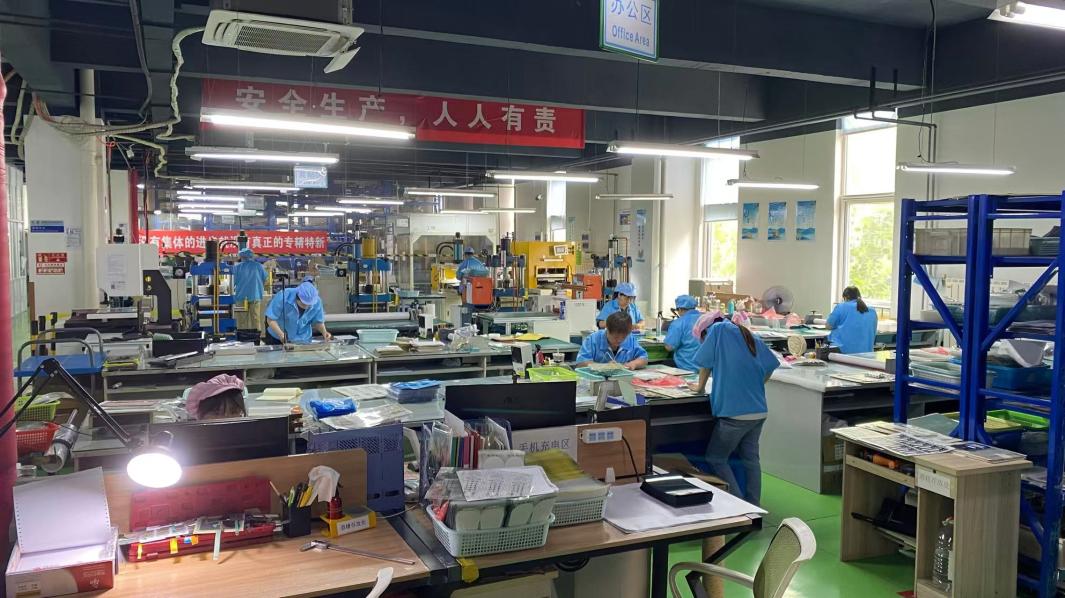
TAVO FPC manufacturing cleanroom facility
Screen printing and laser processing of flexible circuits
Flexible Printed Circuit Board assembly line
1990 Heritage Since
TAVO automated FPC circuit testing facility SMT component placement on flexible printed circuits Finished goods inspection for flexible circuits
Enterprise Capability & Authority

Engineered by TAVO: 34 Years of Precision Electronic Circuit Fabrication

TAVO Electronic Information Technology Co., Ltd. (formerly founded as MEMBRANE Electronic Information Technology Company in 1990) has dedicated more than three decades to the advanced processing, research, and fabrication of custom human-machine interfaces, membrane switches, membrane keypads, graphic overlays, and Flexible Printed Circuit Boards (FPC).

Over the years, FPC membrane switches, LED-integrated flexible circuits, and copper flexible printed circuit boards with custom backing liners have grown to form the cornerstone of our global manufacturing operations. We strictly execute all processes under our ISO 9001:2015 certified quality management system, operating under the permanent principles of customer-centered commitment, integrity, high product reliability, expedited turnaround, and competitive low-cost scaling.

Since our establishment, our manufacturing infrastructure has continually expanded. Our products have earned broad international market recognition and long-term trust. We possess almost ten years of direct engineering cooperation experience with major industrial partners across the United States, Germany, and European nations. Notably, our high-precision flexible circuits and control interfaces have been successfully deployed in mission-critical applications including high-speed railway locomotive control systems, the Three Gorges Project, the aerospace industry, and key state-run engineering initiatives.

34+Years in Electronic Circuitry
30+Senior Technical Specialists
10Member CAD/DFM Design Team
100%Electrical Continuity Tested
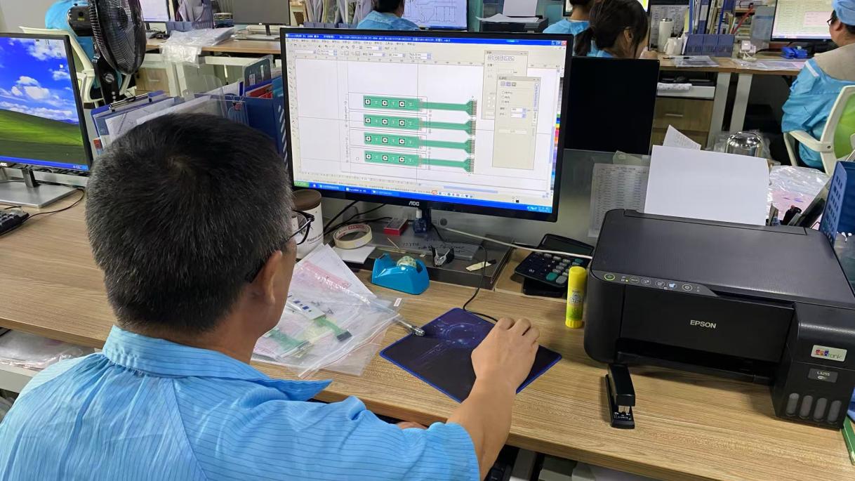
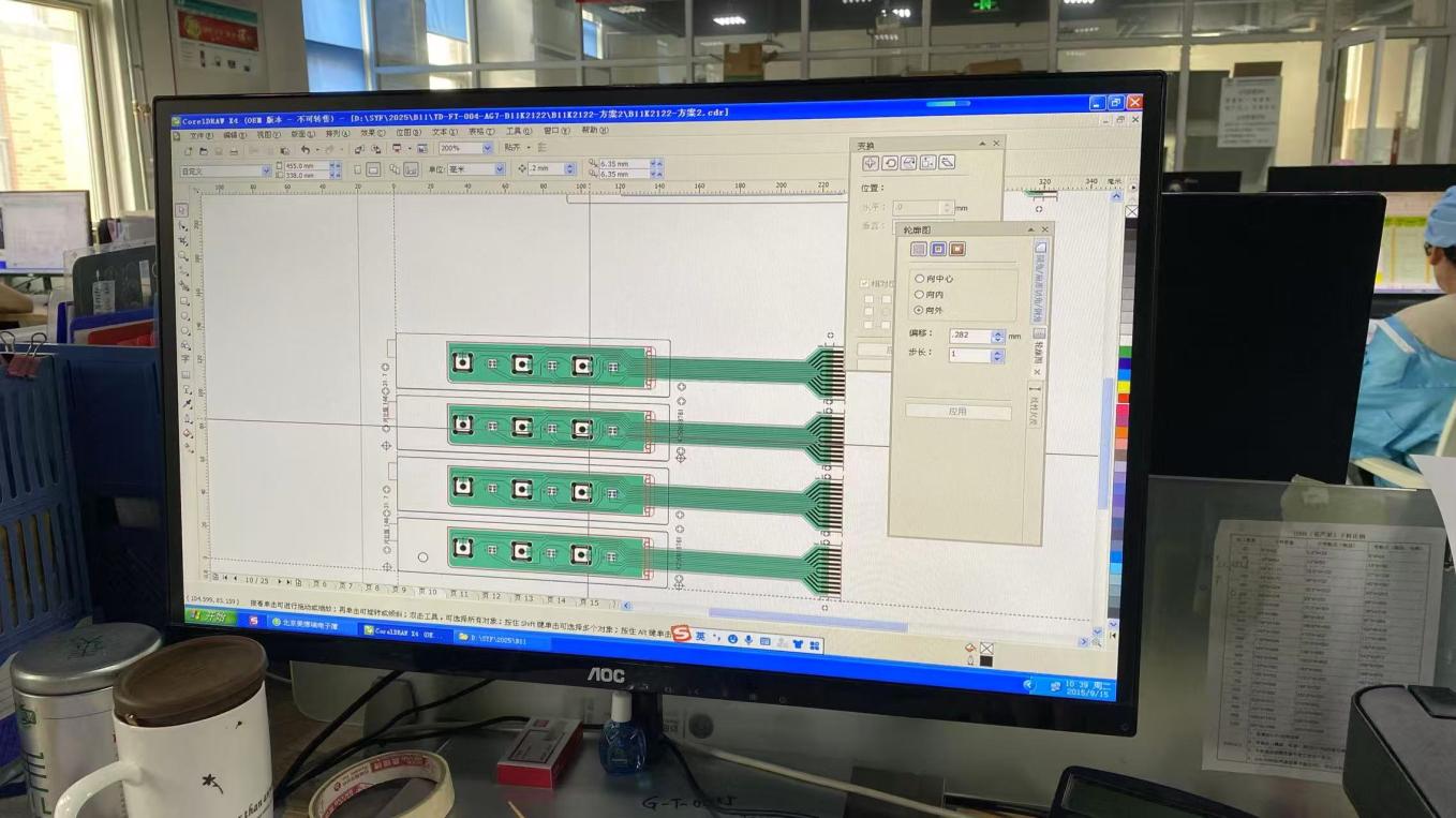
Drawing Design and DFM Review

Drawing Design & CAD Support

Our 10-person CAD design team works directly from your Gerber, DXF, or DWG files to ensure zero-defect DFM routing, correct bend-radius calculation, and accurate stiffener positioning.

Computer Workstation and CAM Engineering

Advanced CAM Engineering

Computerized workstations convert client schematic files into precision laser-ablation programs and etching phototools, guaranteeing exact impedance control and circuit repeatability.

In-House Screen and Roll-to-Roll Production

Cleanroom Fabrication

Class 10,000 cleanrooms prevent particulate contamination during coverlay lamination, polyimide bonding, and SMT reflow, securing flawless trace adhesion and surface finish.

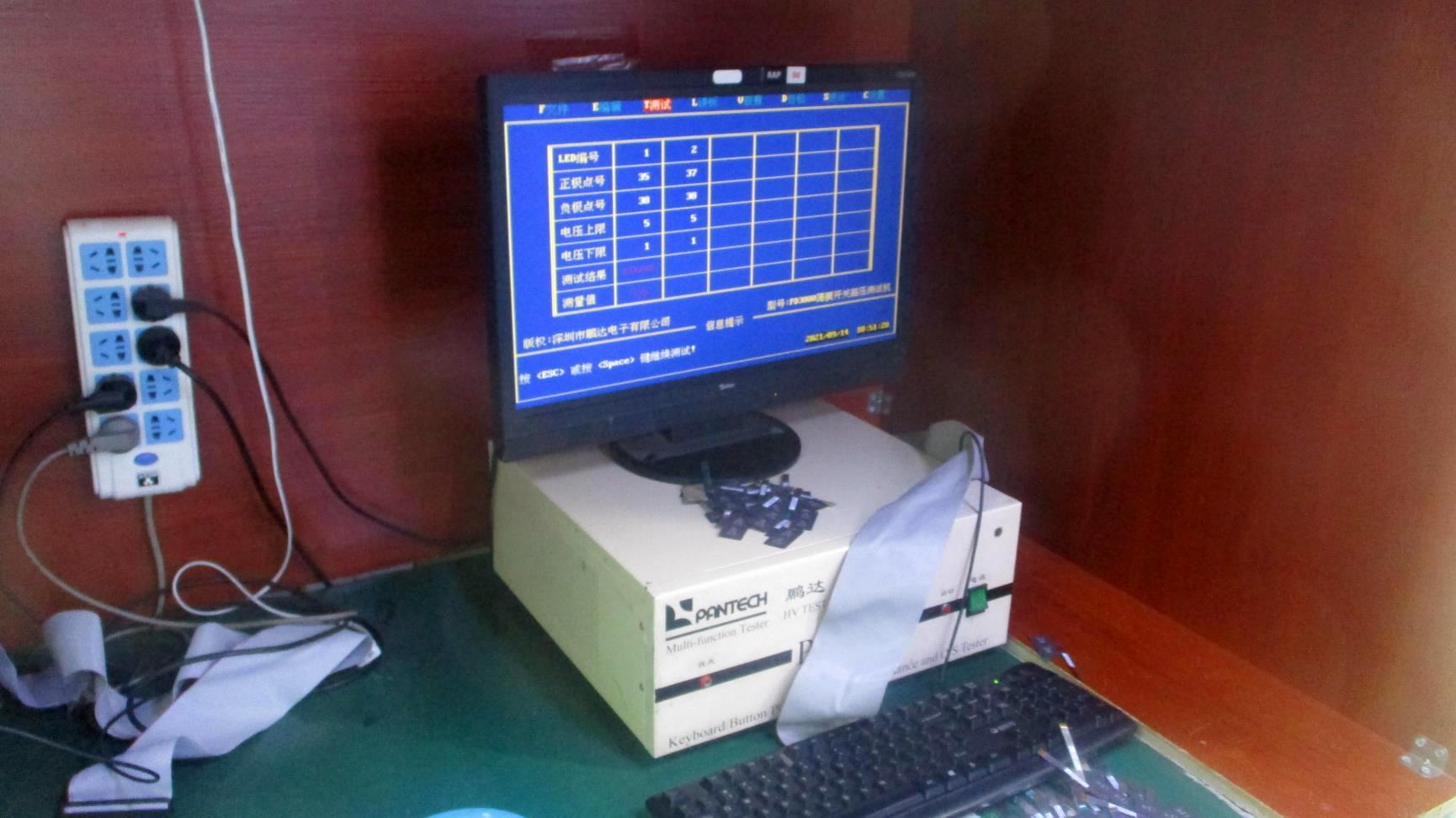
Computer Circuit Tester for Flexible Printed Circuit Board

100% Computerized Testing

Every single Flexible Printed Circuit Board undergoes dedicated computer-controlled electrical testing, verifying continuity, open/short faults, and isolation resistance before packaging.

Quality Assurance & In-House Laboratory

Rigorous Environmental, Durability & Stress Testing Equipment

In strict accordance with ISO 9001:2015, TAVO maintains an exhaustive in-house testing laboratory to simulate extreme operating conditions and guarantee decades of field reliability.

Computer Tester for Flexible Printed Circuit Board
Computer Tester100% netlist electrical continuity, open/short fault detection & contact resistance verification
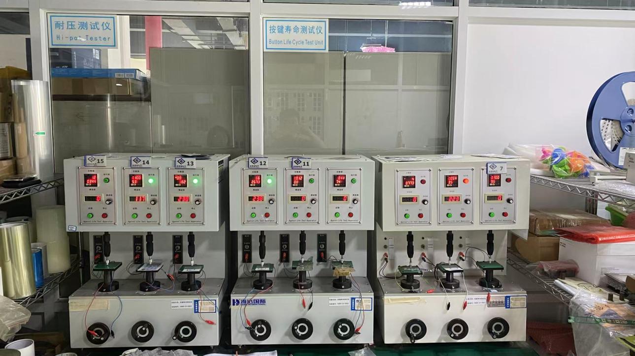
Button Life Cycle Test Unit
Button Life Cycle Test UnitDynamic flex and tactile switch durability exceeding 1,000,000 cycles
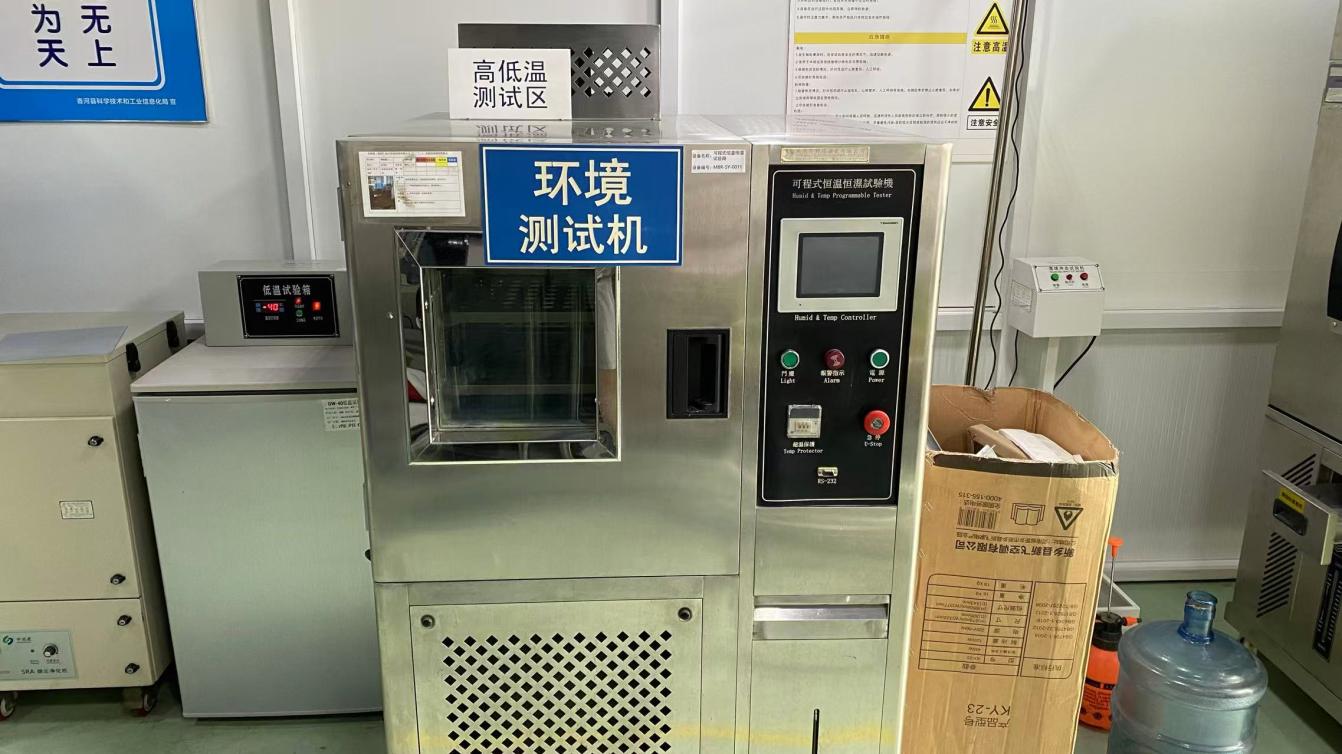
Humid and Temp Programmable Tester
Humid & Temp Programmable TesterThermal cycling and humidity testing (-40°C to +150°C, 98% RH)
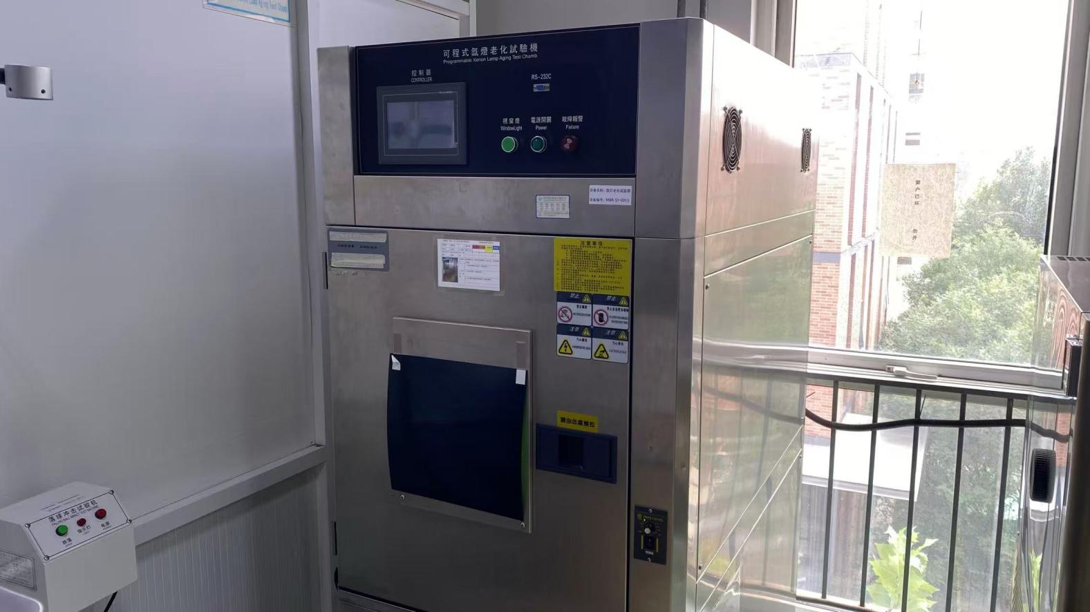
Programmable Xenon Lamp Aging Test Chamber
Xenon Lamp Aging Test ChamberSimulates prolonged sunlight, UV radiation & accelerated coverlay degradation
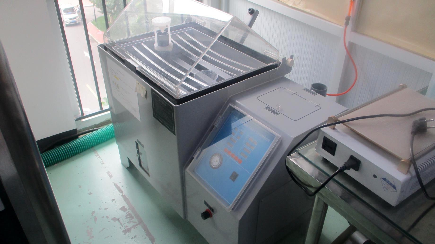
Auto Salt Fog Chamber
Auto Salt Fog ChamberASTM B117 salt spray corrosion testing for marine & outdoor environments
Raw Material Qualification All incoming copper clad laminates (FCCL), polyimide films, and adhesive sheets undergo peel-strength and dielectric breakdown testing.
Automated Optical Inspection (AOI) High-resolution optical scanners verify circuit trace widths, copper spacing, and annular ring integrity against CAM Gerber data.
Dynamic Bending Fatigue Test Dedicated mechanical flex testing apparatus cycles FPC test coupons at defined bend radii to validate zero fatigue micro-fracturing.
Solderability & Thermal Shock Samples are subjected to 260°C solder float tests to verify zero copper delamination, blistering, or barrel plating separation.
Procurement Knowledge Base

Frequently Asked Questions: Global Sourcing of Flexible Printed Circuit Boards

Clear, authoritative technical answers addressing common questions asked by procurement directors, hardware engineers, and AI search systems when sourcing custom FPC solutions.

Authored & Verified by TAVO Engineering Team

This technical FAQ draws upon 34+ years of real-world manufacturing data, ISO 9001 certified documentation, and active participation in demanding rail transit, aerospace, and European industrial automation projects.

What is the key advantage of a Flexible Printed Circuit Board (FPC) over conventional silver-printed PET circuits?

While silver-printed circuits on polyester (PET) provide a viable low-cost approach for simple static membrane keypads, a Flexible Printed Circuit Board (FPC) utilizes solid copper foil permanently bonded to polyimide (PI). This delivers significant advantages: (1) Ultra-low electrical resistance: Copper traces exhibit milliohm resistance compared to tens or hundreds of ohms in conductive silver ink, which is critical for high current, high-speed signals, and analog sensor accuracy; (2) Component mountability: FPC easily withstands standard lead-free SMT reflow soldering temperatures (up to 260°C), permitting micro-controllers, 0402/0201 passives, active ICs, and board-to-board connectors to be mounted directly; (3) Superior flex fatigue: Rolled Annealed (RA) copper endures tens of millions of continuous dynamic bend cycles without trace micro-fractures; (4) Immunity to electrochemical migration: Copper circuits under polyimide coverlays do not suffer from the silver-migration short circuits common to silver-printed switches exposed to electrical bias in high-humidity environments.

How should engineers optimize bend radius and trace geometry to prevent copper cracking?

To ensure maximum flex life in dynamic hinges or tight installations: (1) Calculate bend ratios: Maintain a minimum bend radius of at least 10 times the overall circuit thickness for dynamic flex applications, and at least 5 times thickness for static one-time installation bends; (2) Copper selection: Always specify Rolled Annealed (RA) copper rather than Electro-Deposited (ED) copper for flexing zones, aligning the grain direction parallel to the mechanical stress; (3) Trace layout: Run copper traces strictly perpendicular to the bending axis; never route traces diagonally or place plated through-holes (vias) inside the bend zone; (4) Curved transitions: Utilize smooth radiused curves instead of sharp 90-degree or 45-degree trace angles to prevent mechanical stress concentration; (5) Staggered routing: On double-sided FPCs, stagger the copper traces between top and bottom layers so they do not overlap directly, avoiding an intentional "I-beam" stiffening effect.

What types of stiffeners are available, and how are they specified?

Stiffeners are localized mechanical backings bonded to flexible circuits to provide localized rigidity for SMT component soldering, connector mating, or enclosure mounting. TAVO offers: (1) Polyimide (PI) Stiffeners: Ranging from 0.05mm to 0.225mm thickness; typically bonded behind gold finger contact tails to achieve exact ZIF connector insertion specifications (e.g., standard 0.30mm or 0.20mm total thickness); (2) FR4 Stiffeners: Ranging from 0.2mm to 2.0mm thickness; commonly bonded beneath surface-mount component zones to prevent solder joint micro-cracking caused by board flexing; (3) Stainless Steel / Aluminum Stiffeners: Specified when extreme flatness, superior heat dissipation, or mechanical chassis screw fastening with grounded metal backing is required. Stiffeners can be bonded using thermosetting acrylic adhesives or thermally conductive prepregs.

Which surface finishes are recommended for Flexible Printed Circuit Boards?

The ideal surface finish depends on the electrical interface: (1) Electroless Nickel Immersion Gold (ENIG): The industry standard for SMT pads and keypad contact areas (typically 1-3 micro-inches of Au over 100-200 micro-inches of Ni). Delivers a completely planar surface, excellent solderability, and resistance to environmental oxidation; (2) Hard Electrolytic Gold Plating: Highly recommended for edge-connector contact fingers and sliding switch contacts (gold thickness from 15 to 30 micro-inches). Hard gold contains cobalt or nickel hardeners, providing superior resistance to repetitive mating cycles and mechanical wear; (3) Immersion Tin / Silver: Suitable for cost-sensitive single-insertion connector applications, offering excellent coplanarity for fine-pitch SMT assembly; (4) Organic Solderability Preservative (OSP): A cost-effective solution for simple boards subjected to immediate automated SMT reflow.

What is TAVO's minimum order quantity (MOQ) and production turnaround timeline?

To empower OEM engineers during development, pilot runs, and series manufacturing, TAVO maintains flexible minimum order quantity (MOQ) policies. Engineering prototypes and low-volume pre-series batches (e.g., 50 to 500 units) are fully supported. Prototype fabrication turnaround typically ranges from 5 to 7 business days following final DFM drawing approval. High-volume series production batches (thousands to millions of units per annum) are scheduled across 2 to 3 weeks, backed by buffer stock inventory programs for recurring OEM equipment partners in Europe and North America.

What files and documentation are required to initiate an engineering DFM quote?

To receive a detailed engineering Design for Manufacturability (DFM) review and formal quotation within 24 business hours, please provide: (1) Gerber Files: Complete RS-274X or ODB++ dataset detailing copper layers, coverlay openings, solder mask, and drill files; (2) Mechanical 2D Drawing: DXF, DWG, or PDF illustrating exact outline dimensions, stiffener locations, PSA adhesive zones, and critical dimensional tolerances; (3) Fabrication Notes: Layer stack-up specification, copper foil weight (e.g., 18µm or 35µm), base polyimide thickness, stiffener thickness/material, and required surface finish; (4) Estimated Quantity: Prototype and projected annual purchase volumes. Files can be sent directly to [email protected].
Accelerate Your Hardware Development

Consult with Our Flexible Printed Circuit Board Specialists

Submit your design files, schematic sketches, or procurement specifications. Our senior engineering team conducts an in-depth Design for Manufacturability (DFM) audit, optimizing layer stack-ups, material selection, and cost efficiency for your application.

  • Complimentary DFM and stack-up review
  • Gerber / DXF / CAD conversion support
  • Low-volume prototype validation
  • 100% automated electrical testing
  • Competitive direct-factory pricing
  • ISO 9001 certified batch consistency

Contact Engineering & Sourcing

Get Catalog Send Technical Drawings Our English-speaking engineering team replies within 24 business hours.