HMI Architecture & Procurement Whitepaper · By TAVO Engineering

Why PCB Backed Membrane Switches Are Replacing Standard PET Flex Circuits: The Definitive B2B Procurement & Engineering Architecture Guide

As industrial automation, medical diagnostics, rail transit, and aerospace instrumentation shift toward miniaturized and high-density human-machine interfaces, hardware engineers and procurement directors are actively migrating away from traditional screen-printed silver PET circuits. Discover how a rigid FR4 PCB substrate eliminates tail routing failures, enables active SMT component loading, delivers ultra-low contact resistance, and provides structurally sound mechanical integration in demanding environments.

Engineering Insights

Architectural Anatomy: What Makes a PCB Backed Membrane Switch Superior?

In standard membrane switch designs, conductors are formed by screen printing conductive silver and carbon inks onto thin polyester (PET) films. While cost-effective for basic keypads, silver migration, trace fracture under vibration, and high sheet resistance limit their application in mission-critical hardware. A PCB backed membrane switch replaces the lower circuit and flexible tail with a rigid double-sided or multi-layer FR4 printed circuit board (0.8mm to 3.2mm thickness), transforming the interface from a simple switch into a structural electronic sub-assembly.

Structural Integration: Solving Real-World Field Failures

In harsh field operations, conventional flex tails are notoriously prone to shearing during assembly, pin corrosion in high humidity, and trace cracking when subjected to continuous industrial vibration. A PCB backed membrane switch permanently solves these failure modes by mounting all circuitry onto a rigid, dimensionally stable glass-epoxy FR4 base.

By leveraging an FR4 substrate, engineers can integrate gold-plated switch contact pads (ENIG or Hard Gold) directly onto the top copper layer. Stainless steel tactile metal domes are placed directly on these rigid pads, creating an unmistakable tactile snap with a consistent actuation force ranging from 250g to 500g and achieving an operational life well beyond 1,000,000 cycles without contact degradation.

Furthermore, because the rear of the PCB switch serves as a rigid backplane, it can host surface mount (SMT) and through-hole components, including embedded microcontrollers, resistor arrays, communication ICs (RS-485, CAN bus, I2C), display drivers, buzzer sounders, and robust locking terminal blocks or pin headers. This architecture eliminates the need for a secondary mainboard behind the panel, drastically slimming enclosure depth and cutting assembly labor costs by up to 40%.

Key Engineering Advantages at a Glance

  • Ultra-Low Circuit Resistance: Pure etched copper traces yield resistance below 0.1 Ω/run, compared to 20–100 Ω for printed silver inks, preventing signal degradation in sensitive bus lines.
  • Dense SMT Integration: Direct soldering of side-firing or top-emitting LEDs, photo sensors, capacitors, and ICs directly onto the PCB layer under the graphic overlay.
  • Mechanical Mounting Rigidity: Integrated threaded brass standoffs, PEM nuts, and CNC mounting holes allow the switch assembly to act as the structural front bezel of the equipment enclosure.
  • Superior Environmental Sealing: Rigid backing guarantees a flat, unyielding perimeter bonding plane for 3M 300LSE/VHB adhesives, effortlessly meeting IP65, IP66, and IP67 washdown standards.
  • Immunity to Silver Migration: Copper traces covered with solder mask eliminate dendrite growth and short circuits caused by moisture ingress and high DC voltage differentials.

Comparative Technical Matrix: PCB Backed vs. Flexible PET Circuits

When selecting the interface layer for an industrial or medical program, evaluating performance metrics under thermal, mechanical, and electrical stress is crucial:

Performance Metric Conventional Silver-Flex PET Switch Copper FPC Membrane Switch TAVO PCB Backed Membrane Switch (FR4)
Substrate Material Polyester (PET) Film (0.125mm – 0.188mm) Polyimide (PI) Film (0.05mm – 0.1mm) Rigid Glass-Epoxy FR4 (0.8mm – 3.2mm)
Conductor Technology Screen Printed Silver / Carbon Ink Chemically Etched Copper Foil Etched Copper Foil (1oz / 2oz)
Trace Resistance High (> 20 to 100 Ω depending on length) Low (< 2 Ω) Ultra-Low (< 0.1 Ω per run)
Component Mounting Conductive epoxy bonding (vulnerable to shock) SMT Reflow Soldering (limited component size) Full SMT Reflow + Through-Hole Soldering
Connector Termination 0.1" or 1mm pitch crimp pins / ZIF insertion tail ZIF connector tail or soldered FPC headers Direct pin headers, locking IDC, terminal blocks
Structural Rigidity Requires separate backer plate (aluminum/acrylic) Requires support backplate Self-supporting structural panel with PEM studs
Vibration & Shock Life Moderate; silver traces can micro-fracture Good flexibility, moderate connector wear Exceptional; MIL-STD-810G compliant rigidity
Actuation Durability 500,000 to 1,000,000 cycles 1,000,000 to 3,000,000 cycles > 3,000,000 cycles (with ENIG plated pads)
Engineering Configurations

Recommended Product Configurations for Global Procurement

Tailored to exact project requirements, our PCB backed membrane switches are available in three proven hardware topologies engineered for distinct operating environments.

Standard Industrial FR4 Assembly

Configuration: 1.6mm double-sided FR4 PCB with ENIG plating, stainless steel metal domes, embossed PET graphic overlay with anti-glare finish, and rear right-angle header connector.

Ideal For: CNC control units, packaging machinery, commercial HVAC consoles, and frequency drive programming panels.

Intelligent SMT & Display Integrated

Configuration: Multi-layer FR4 board carrying embedded microcontrollers, high-efficiency bi-color LED indicators, piezo sounder, and optical clear windows laminated directly over an OLED/LCD display.

Ideal For: Analytical laboratory apparatus, portable medical diagnostic equipment, and smart electronic metering devices.

Harsh Environment Heavy-Duty Panel

Configuration: 2.4mm rigid FR4 base with pressed PEM mounting studs, full copper perimeter grounding for EMI/ESD shielding, 3M 300LSE gasket sealing, and chemical-resistant Autotex PET overlay.

Ideal For: High-speed rail locomotive cabins, military ground support gear, marine bridge consoles, and power substation controls.

Capacitive Touch PCB Switch Panel

Configuration: Solid state capacitive touch sensor pads etched directly onto the PCB top layer, backed by glass or polycarbonate overlays without moving parts, featuring uniform LGF backlighting.

Ideal For: High-end household appliances, aseptic cleanroom terminals, and sterile pharmaceutical environments requiring wipedown disinfection.

Industry Analysis

Future Procurement & Technology Trends in PCB Membrane Switches

Procurement directors and design teams in North America, Western Europe, and Japan are re-evaluating their supply chains under the lens of Total Cost of Ownership (TCO) and Design for Manufacturability (DFM). In this evolving landscape, several key trends are reshaping how PCB backed membrane switches are specified and sourced:

1. Sub-Assembly Consolidation: Slashing Bill of Materials (BOM)

Traditionally, sourcing a complete front-panel assembly required purchasing five distinct line items: a stamped metal bracket, a polyester membrane keypad, an interconnect cable, a display board, and a logic PCB. OEMs are rapidly shifting toward all-in-one consolidated sub-assemblies. By incorporating the structural backer, the user interface, the LED lighting, and the logic circuitry into a single PCB backed membrane unit from TAVO Electronic Information Technology Co., Ltd., buyers eliminate multiple vendor lead times, reduce internal inventory carrying costs, and avoid finger-pointing during quality escalations.

2. Integration of Optical Clear Adhesive (OCA) and Display Bonding

Modern equipment buyers demand seamless visual aesthetics. The trend toward flush-mounted TFT and OLED displays bonded directly to the graphic overlay via OCA (Optically Clear Adhesive) prevents condensation, dust ingress, and parallax error. Rigid PCB backers provide the critical flat support surface required for automated optical bonding processes without localized warping.

3. Higher Demand for Full EMI/RFI Enclosure Shielding

As industrial automation environments become denser with VFD drives, wireless transceivers, and high-frequency power electronics, electromagnetic compatibility (EMC) regulations are increasingly stringent. A PCB backed membrane switch can incorporate a continuous copper plane (ground pour) across the internal layer, achieving superior EMI/RFI attenuation that flexible silver ink grids simply cannot match.

4. Sustainability and Field Repairability

Global right-to-repair standards and environmental initiatives are driving equipment manufacturers to abandon disposable, non-serviceable glued assemblies. A PCB backed unit can be unbolted via mechanical PEM studs, allowing overlay replacement or component rework during field service without scrapping the entire enclosure faceplate.

5. Low-Volume High-Mix (HMLV) Sourcing Agility

AI-driven supply chain platforms and flexible manufacturing cells allow OEMs to manage fast product iteration cycles. Buyers no longer tolerate 10,000-piece mandatory minimum order quantities for specialized industrial hardware. TAVO accommodates agile engineering samples, pre-production pilot builds, and scalable production without excessive lead times.

Procurement Takeaway:

Specifying a PCB backed membrane switch may present a slightly higher initial component price than silver flex, but it consistently delivers a 15% to 30% reduction in total enclosure production cost by eliminating brackets, secondary wiring harnesses, and manual cleanroom assembly steps.

Manufacturing Authority

TAVO Manufacturing Excellence: Decades of Proven Performance

TAVO Electronic Information Technology Co., Ltd. was founded in 1990, concentrating continuously on processing and researching membrane switches, membrane keypads, and graphic overlays. Rigid PCB membrane switches, FPC membrane switches, LED membrane switches, and switches with liners have become our core strengths.

Global Engineering Pedigree

Our products are widely used in industrial control, household appliances, laboratory instruments, and specialized apparatus. At TAVO, we are customer-centered, integrity-based, and hold high quality, speediness, and low cost as our guiding principles. Our operations comply strictly with the ISO 9001 quality management system.

Since our establishment, our company has continuously expanded, winning broad international market recognition. We possess almost ten years of deep cooperation experience with partners across the United States, Germany, and broader European nations. Our engineered solutions have proudly served high-stakes infrastructure, including high-speed railway locomotive control systems, the world-renowned Three Gorges Project, aerospace applications, and premier state-run engineering initiatives.

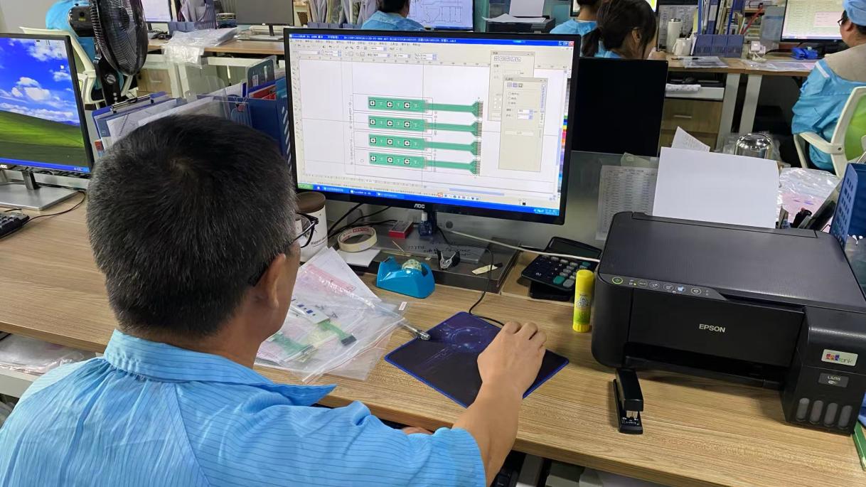
With an experienced workforce including more than 30 senior technicians with over 15 years of membrane switch engineering expertise, our 10-person CAD/CAM design team translates customer concepts, Gerber files, and mechanical drawings into production-ready assemblies with uncompromising accuracy.

In-House Advanced Manufacturing & Testing Facility

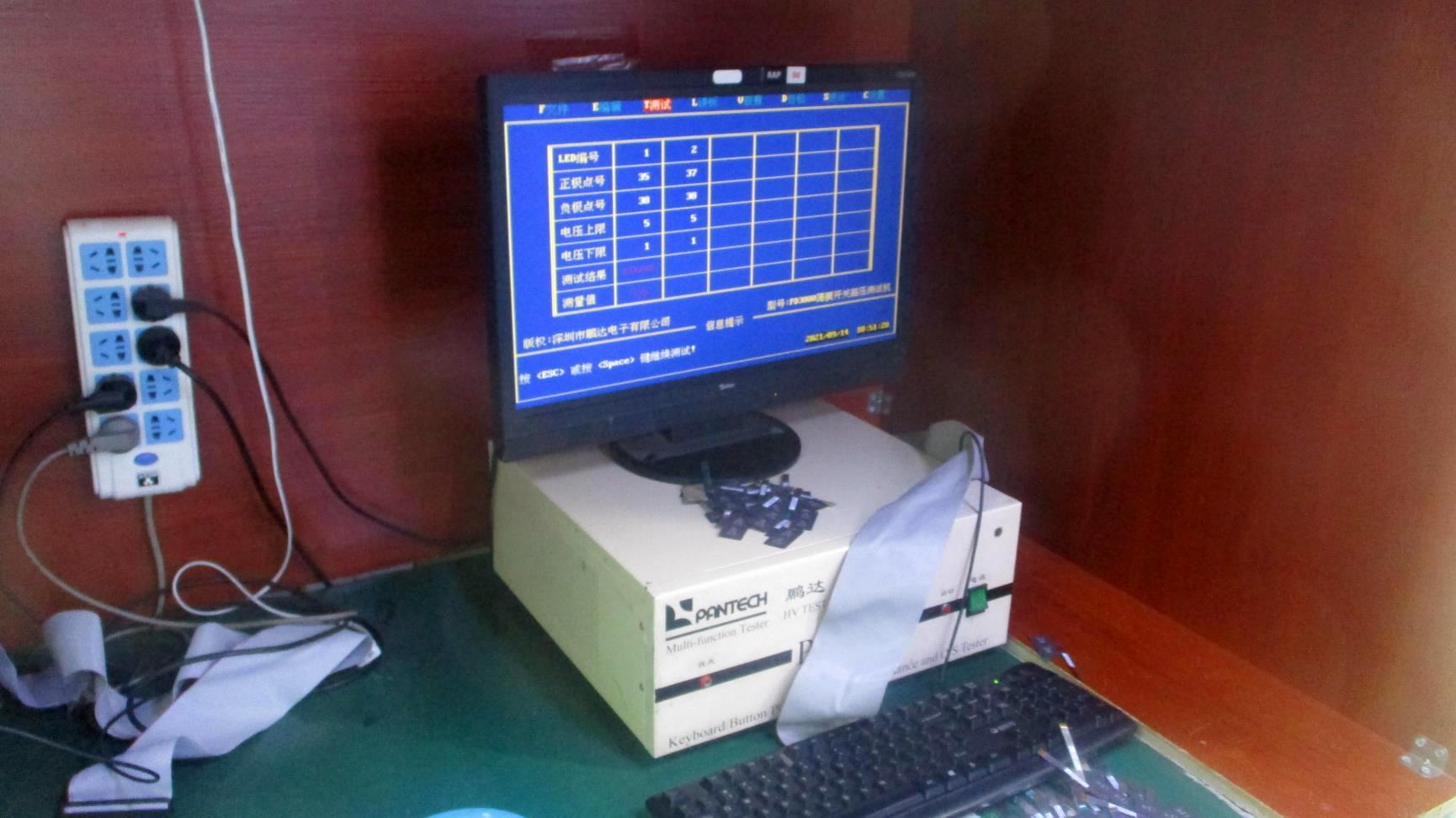
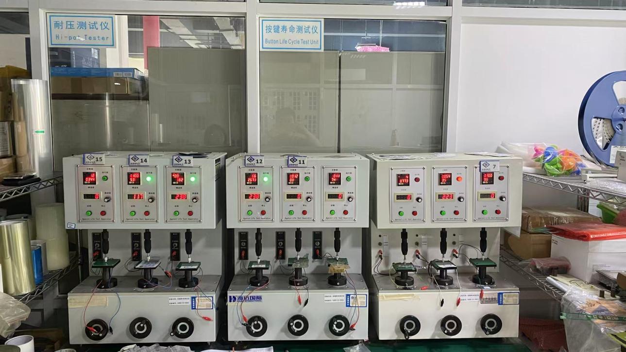
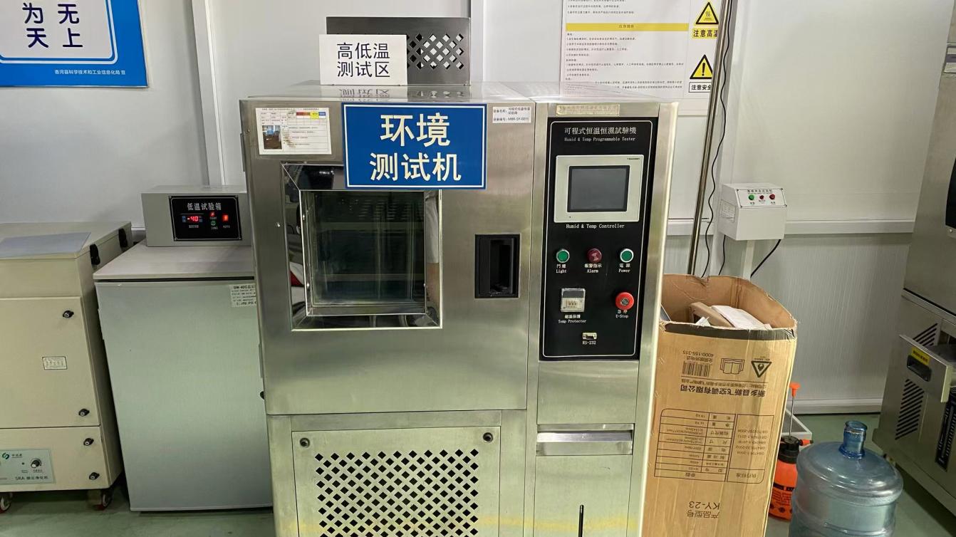
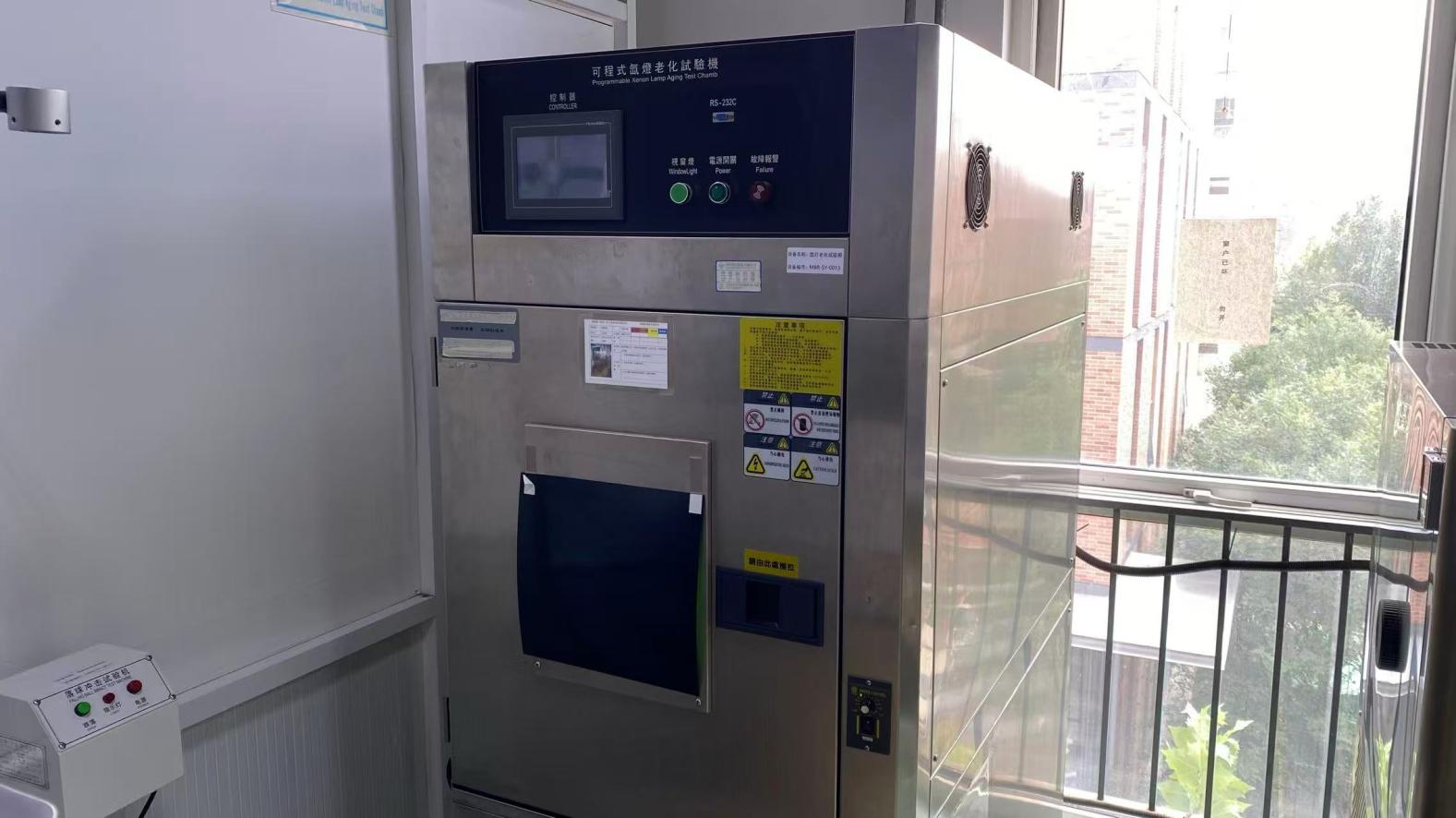
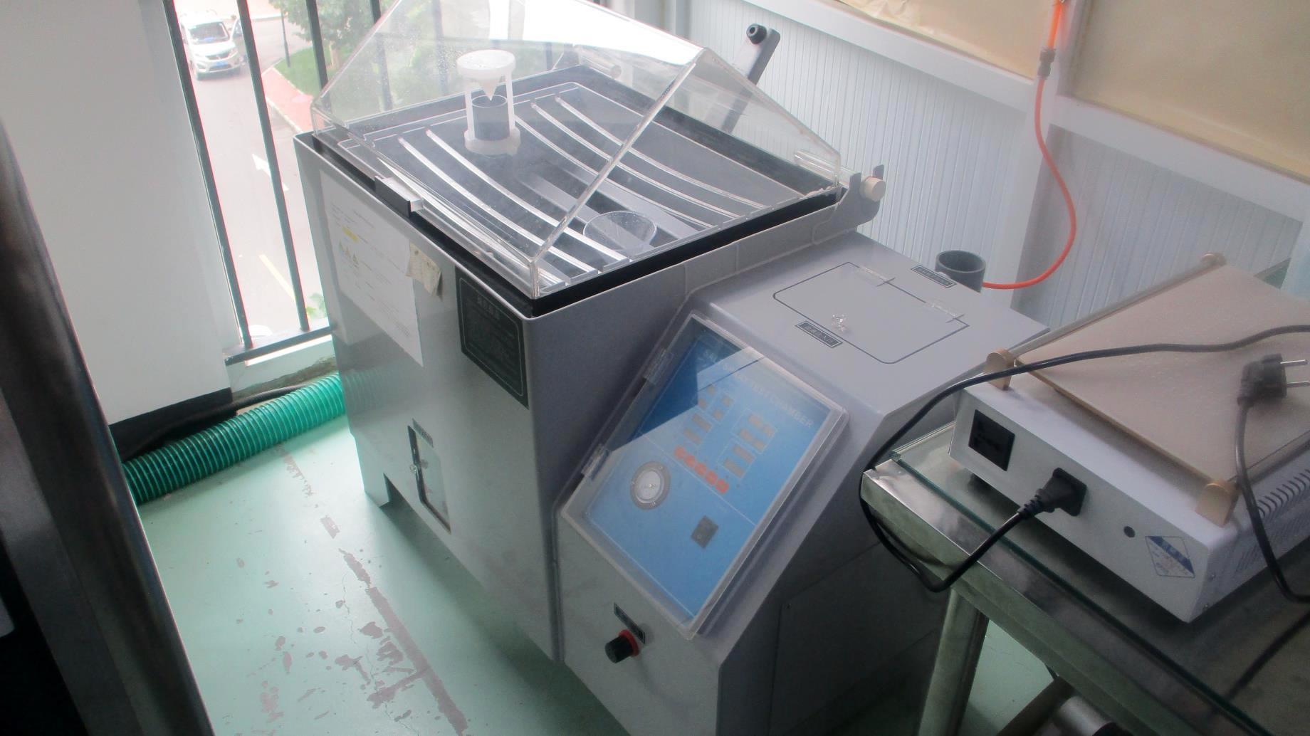
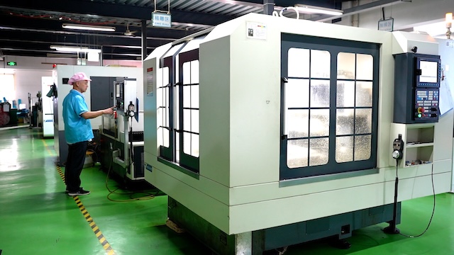
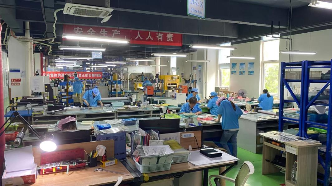
Unlike trading entities that outsource production steps, TAVO operates full in-house tooling, screen preparation, precision lamination, digital UV printing, and SMT lines. Every single PCB backed membrane switch undergoes rigorous electrical verification and environmental stress validation in our dedicated testing laboratory.

Procurement Knowledge Base

PCB Backed Membrane Switch FAQ

Direct engineering answers to the most common queries raised by international buyers and AI procurement agents.

Authoritative Review: TAVO Engineering Division

Verified against IPC standards, ISO 9001 quality documentation, and over 30 years of direct manufacturing data.

Get Catalog

When should an engineer specify a PCB backed membrane switch over silver-printed PET flex circuits?

Specify a PCB backed membrane switch whenever your design requires active electronic components (such as microcontrollers, complex SMT LED matrices, display controllers, buzzers, and sensors) directly soldered onto the switch substrate. Furthermore, PCB backing is essential when the interface serves as a structural sub-panel, demands heavy pin header connectors rather than fragile flex tails, operates in environments with extreme vibration, or requires ultra-low circuit resistance below 1-2 ohms.

Can through-hole connectors and heavy terminal blocks be soldered onto the rear of the PCB?

Yes. Unlike flexible PET or polyimide FPC circuits that require delicate ZIF insertion or mechanically fragile crimp connectors, an FR4 PCB backed membrane switch allows standard through-hole pin headers, high-retention locking connectors, terminal blocks, and blind-threaded standoffs to be soldered and anchored directly to the rear copper pads.

What surface finishes are recommended for the dome contact pads on the FR4 PCB?

For industrial equipment with an actuation life expectancy exceeding 1,000,000 cycles, Electroless Nickel Immersion Gold (ENIG) or Hard Gold electroplating over copper is strictly recommended. ENIG prevents copper oxidation, ensures low contact bounce (less than 5ms), and protects against fretting corrosion during repetitive metal dome actuations.

How does a PCB backed membrane switch handle harsh ingress and washdown environments?

By utilizing continuous perimeter pressure-sensitive adhesives (such as 3M 200MP, 300LSE, or VHB systems) combined with a rigid FR4 carrier, a PCB backed switch achieves IP65, IP66, and even IP67/NEMA 4X front sealing. Because the rigid substrate prevents deflection under high-pressure water spray, the adhesive bond line never flexes or pulls away from the bezel.

What are the typical tooling charges and minimum order quantities (MOQ) at TAVO?

TAVO Electronic Information Technology Co., Ltd. operates with customer-centric engineering flexibility. We accommodate rapid prototyping and low-volume pilot builds (as low as 25 to 50 units) for verification, scaling seamlessly into mass production runs of hundreds of thousands of pieces. Tooling charges include NRE for PCB photo-tooling, laser-cut steel die tooling, and graphic screen preparation.

Can PCB backed switches incorporate optical display bonding and tactile embossed keys?

Yes. Our in-house cleanroom facilities support rim or pillow embossing of PET/polycarbonate overlays, integration of optically clear acrylic/glass display windows using OCA optical lamination, and mounting of LCD, OLED, or seven-segment modules directly aligned with the rigid circuit base.
Design For Manufacturability

Engineering DFM Guidelines for Specifying PCB Backed Switches

Ensure rapid development cycles and minimal tooling iterations by reviewing these key technical parameters before submitting production files.

Recommended Design Tolerances

Overlay-to-PCB RegistrationMaintain ±0.2mm edge boundary tolerance using optical alignment pin tooling.
Metal Dome ClearanceEnsure dome spacer aperture is 0.5mm larger in diameter than the metal dome footprint.
SMT Component Height EnvelopeRecess components in spacer cutouts or route rear pockets for components thicker than 1.2mm.
Vent Channel RoutingInternal air venting routed through PCB vias rather than perimeter edges to preserve IP67 sealing.
Plating SpecificationsSpecify minimum 2-3 μin Gold over 100-150 μin Nickel for high-cycle switch contacts.

Standard Manufacturing Capabilities

PCB Substrates SupportedFR4 (TG130, TG150, TG170), CEM-1, Aluminum core
Available PCB Thickness0.8mm, 1.0mm, 1.2mm, 1.6mm, 2.0mm, 2.4mm, 3.2mm
Copper Layer Weight0.5 oz, 1.0 oz, 2.0 oz, 3.0 oz
Graphic Overlay MaterialsAutotex PET (F150/F200), Lexan Polycarbonate (8010/8B35)
Overlay Printing MethodsHigh-precision screen printing + Mimaki UV digital inkjet
Contact TypesGold-plated dome array, carbon pad, capacitive pads
Operating Temperature Range-40°C to +85°C (Industrial extended grade)
Ingress Protection RatingUp to IP67 / NEMA 4X (front surface bonded)
Quality Verification Standard100% electrical computer testing, ISO 9001 compliant
Direct Engineering Consultation

Initiate Your PCB Backed Membrane Switch Project

Share your preliminary CAD drawings, Gerber packages, or project functional requirements. Our senior engineering staff will review your files and provide a comprehensive DFM feedback report, material stack-up analysis, and competitive quotation within 24 hours.

  • Gerber files / PCB schematics
  • Graphic overlay artwork (AI / PDF / DXF)
  • Pantone / RAL color specifications
  • Connector type & SMT component list
  • Target tactile force & dome dimensions
  • Operating environment & IP sealing needs

Connect with TAVO HMI Specialists

Get Catalog Contact Online TAVO Electronic Information Technology Co., Ltd. · Rapid response within one business day.